

Spintronics
Orion and ATC Sputtering Deposition Systems

Overview
Spintronics denotes the field of electronics that specifically leverages the spin of the electron to enhance the performance of devices. Both computer memory and logic devices are being envisioned and developed, fueled by society’s ever-increasing need for computational power. Spintronics devices offer capabilities such as high data recording density, non-volatility, stronger electronic and magnetic responses which are also tunable, or hardening against radiation or magnetic fields. Spintronic devices are already serving to extend device performance in accord with the famous Moore’s Law. Continued vigorous research efforts strive to discover new configurations and optimize existing ones for commercialization.
Spintronics can be understood by considering some effects and devices that depend on spin for their operation. A sampling of these is listed below. Some have been commercialized, while others are still in the research and development stage – and all of them depend on thin film deposition technology to bring them to realization.
Giant Magnetoresistance (GMR). This effect arises when a non-magnetic metal film is sandwiched between two ferromagnetic (FM) layers. If the FM layers’ magnetic moments are aligned in parallel, the partially spin-polarized current from the first FM layer experiences a different amount of scattering (usually lower) in the second layer, as opposed to if they are anti-parallel. This effect has been used in magnetic disk drive read heads as a sensor to detect the data written into the drive platter (i.e. the “ones and zeros”.)
Tunneling Magnetoresistance (TMR). This is similar to GMR but with an insulating layer between the two FM layers. This increases the size of the effect (percent change in resistance). These are still being used as read-head sensors. Continued R&D to increase the size of the effect allows the heads to decrease in size, supporting higher data storage density.
Magnetic Tunnel Junction (MTJ). This is a variation of a TMR device, which is being used as a memory device. A reference FM layer is “pinned” so that its magnetization will not flip under the influence of a writing magnetic field. Flipping a second, free layer changes the resistance of the MTJ, providing two states that can encode computer ones and zeros. In the MTJ sketch below, higher data density is achieved by having the magnetization perpendicular to the film surface (pMTJ).
Exchange Bias. Coupling an antiferromagnetic (AM) thin film layer to an FM layer is a method to create the pinning effect in MTJ’s, so that the free layer can be written (which is accomplished by a variety of effects such as those mentioned below).
Magnetoresistive Random Access Memory (MRAM). This thin-film based product incorporates large arrays of MTJ’s to create high speed, non-volatile computer memory. The bits can be written with a magnetic field (Toggle MRAM) or by other physical effects; two examples are listed below.
Spin Transfer Torque MRAM (STT-MRAM). This type of memory, already commercialized as well, does not require the application of a magnetic field to flip the free FM layer. Rather, a spin-polarized current is passed through the MTJ to carry out the write operation. A commercial STT-MRAM product (Everspin Technologies) is shown here.
Spin-Orbit Torque MRAM (SOT-MRAM). This technology, currently in development, utilizes a current passing parallel to the MTJ layer stack, rather than through it. SOT-MRAM offers the promise of high durability and GHz switching speed.
Magnetic Heusler Alloys. These three-element intermetallic compounds are being widely investigated for their tunable magnetic properties, which could be valuable in spintronics. Co-deposition by sputtering is a flexible and rapid method to fabricate these alloys across the ternary phase space.
All of the above materials and devices are primarily developed and manufactured in thin-film form. A highly flexible R&D sputter deposition tool is ideal for exploring the wide combination of thin film stacks found in spintronics devices.

GMR, TMR Structures with Perpendicular Magnetic Anisotropy

Exchange-Biased pMTJ

STT-MRAM
Key Features of the Orion and ATC Sputtering Systems For Spintronics
Magnetron Sputtering Sources:
AJA International offers the best sputtering performance in the industry for magnetic materials used in spintronics devices. Each system offers configurations for mounting several magnetrons, in either sputter up or sputter down configurations. The ATC Series can support up to 13 guns in combinations of confocal, direct, and off-axis sputtering geometries for exploring large material spaces. The guns feature integral gas injection rings for local process gas delivery.
Ultra-High Vacuum (UHV) Design:
As film purity is critical in this application, the systems are engineered to achieve base pressures ranging from the low 10⁻⁷ Torr to the low 10⁻¹⁰ Torr regime. Systems can be constructed using all-metal seal vacuum chambers, and in-house manufactured bakeout jackets are available for thorough vacuum conditioning and system degassing.
Power Supply Options:
DC, pulsed DC, RF and HiPIMS supplies can all be configured into the system. AJA’s standard Phase II-Au control system will accommodate up to (5) DC power supplies with integral 4-way switchboxes, (4) RF power supplies, and (1) 4-way RF switchbox. This allows maximum flexibility for sequential or co-deposition from a large selection of sputter guns so that new material systems can be rapidly developed.
Substrate Holder:
The substrate holder is highly configurable, supporting sample sizes ranging from small coupons to full wafers up to 6” (Orion) or 12” (ATC) diameter with excellent film thickness uniformity. Available functionalities include high-temperature substrate heating (up to 800–1,000 °C), cryogenic or water-based cooling (LN₂ or H₂O), azimuthal rotation for uniform film growth, motorized Z-axis motion, and RF/DC substrate biasing for advanced process control.
Process Gas Delivery:
The system supports up to four mass flow controllers (MFCs) for precise regulation of process gases. Typical gases used in epitaxial deposition include Ar, O₂, and N₂, allowing for a wide range of reactive and inert sputtering processes. A gas ring can be provided at the substrate for reactive deposition of oxides and nitrides.
Deposition Recipe Generator:
The software makes it simple to create and store up to 100+ recipes for depositing layer stacks. It is easy to write extensive recipes, and the Excel spreadsheet layout allows line by line layer stacking and review of recipes for accuracy and data extraction if needed. Recipe operation automates the entire deposition process, with auto-abort in case setpoints fail to be reached. Our AJA Excel Spread Sheet Software Emulator makes possible remote recipe creation offline from the system for later import and execution.
Nanometer-Precision Film Thickness Control:
An optional quartz crystal monitor and controller allows calibration of deposition rates. High-stability power supplies provide precise, repeatable deposition rates, while recipe-driven automation ensures accurate, repeatable process execution.
Vertically Integrated System Design:
AJA International manufactures many of the components in the systems. This ensures compatibility and quality, while controlling tool costs. This also speeds up service and provides long service life for the systems.


Performance
Professor Weigang Wang and his laboratory at the University of Arizona have demonstrated many advances in spintronics devices. In an exciting study, they demonstrated voltage-controlled switching of perpendicular magnetic tunnel junctions (pMTJ) which paves the way for more energy-efficient writing, compared to current-controlled switching.
Key to this research was the use of an AJA International advanced UHV sputter deposition system. The group utilized the tool to deposit multi-layered structures with high purity, nanometer-precision thickness, and flat interfaces, to create a unique pMTJ with a rare earth gadolinium oxide (Gd2O3) tunneling layer between CoFeB FM layers.
Their goal was to pave the way to dramatically decrease the energy needed to flip the free layer in the device. Such flipping is typically induced by an electric current, but this requires more energy due to heating effects. The Wang team provided experimental demonstration of two voltage-based effects to change the state of the device – one of the effects being observed for the first time.
Professor Wang’s research shows impressively how the right selection of materials, combined with careful growth conditions, can create new types of devices and open the door to future commercial products that will serve society’s needs for ever-increasing computational power.
Read more on Professor Wang’s work here:
Ultra-Low Energy Magnetization Switching
*Newhouse-Illige, T. et al. (2017). Voltage-controlled interlayer coupling in perpendicularly magnetized magnetic tunnel junctions. Nature communications, 8(1), 15232.
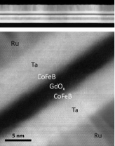
STEM Image of a pMTJ
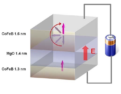
Schematic of a voltage-controlled pMTJ

The AJA International ATC Series Deposition Systems offer a powerful, flexible platform for cutting-edge spintronics research. Engineered to support the precise fabrication of multilayer thin films, these systems are ideal for developing devices based on spin transport and magnetic phenomena. With options for RF/DC magnetron sputtering, in-situ substrate heating, and customized process integration, the ATC Series provides the control and versatility required to advance innovation in magnetic tunnel junctions, spin valves, and related technologies.
To explore how AJA systems can support your spintronics research, contact our sales team today.