

Phase Change Memory (PCM)
Orion and ATC Sputtering Systems For Chalcogenides

Overview
Phase change memory (PCM) is a technology for data storage and computing that relies on reading and writing information to a (typically thin film) material by inducing a change in crystallographic phase. PCM offers a host of unique advantages for both data storage and computing. Research that began in the 1960’s first led to the commercialization of the readable/writeable compact disc (CD R/W, 1997), and intense research efforts continue in academia and industry today.
PCM technology is built on the properties of chalcogenide materials: compounds containing an element from Group 16 of the periodic table, chiefly Selenium (Se) or Tellurium (Te). Chalcogenides can be reversibly switched from amorphous to (poly)crystalline forms, encoding digital information. In CD R/W products, for example, writing via a heat-induced change in the index of refraction of a AgInSbTe glass alters the reflectivity of bits (the 1’s and 0’s) on the disc surface for subsequent reading.
Considering electronic rather than optical memories, a change in resistivity upon the change in form is used to encode information. A current pulse with a short turn-off time heats the material, typically Ge2Sb2Te5 (GST), above its melting point and then quenches it into the amorphous state. Conversely, a lower power pulse with a longer ramp-down time anneals the GST to the polycrystalline form. Referring to the sketch shown here, the amorphous glass state with high resistance represents a digital 0, while the polycrystalline form with lower resistivity represents a digital 1.
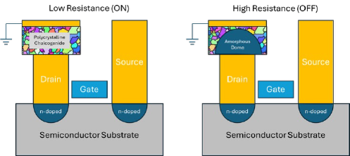
ON and OFF states of a PCM RAM cell
PCM technology boasts several advantages for thin-film-based devices:
Non-volatility. Rather than using charge stored in a capacitor, a PCM RAM stores information in a material phase, which persists even in a power-off state.
Fast switching speed. Devices have demonstrated GHz rates for write (phase change).
Endurance. This represents the number of cycles possible between the high and low states before material degradation. Recent developments have demonstrated that 1011 cycles can be withstood.
High density. Sub-100 nm electrode sizes in PCM could support data density of 1010 bits/cm2.
Long-term stability. GST can maintain its phase – thus its resistivity – stably for more than 10 years at the high service temperatures seen in computing platforms.
Multiple resistance states. Multiple levels of resistance between the high and low states can be stabilized. This can allow more than one bit to be encoded in each cell, further increasing storage density. Variable resistance values can support neuromorphic computing applications, as well.
Breadth of applications. PCM can be utilized for data storage and random-access memories and even in RF switching applications. This opens the door to developing a universal memory material.
These advantages have inspired ongoing thin film device research and product development. Successes have led to estimates of a ten-fold growth in the PCM market over the next decade (Precedence Research).
Key Features of the Orion and ATC Sputtering Systems For Chalcogenides
Magnetron Sputtering Sources:
Each system offers configurations for mounting several magnetrons, in either sputter up or sputter down configurations. The ATC Series can support up to 13 guns in combinations of confocal, direct, and off-axis sputtering geometries for exploring large material spaces and for completing devices with a selection of capping and electrical lead options. The guns feature integral gas injection rings for local process gas delivery. This allows great freedom in exploring composition space and complex device architectures.
Anti-shorting sputtering sources:
Sputtering of chalcogenides is particularly challenging, as material which builds up on the chimney of the sputter gun has a strong tendency to flake, shorting out the anode to the target. Our anti-shorting gun design for chalcogenides shields the anode-target gap, which is proven to allow much longer run times between sputter source cleanings. See the photo below.

Anti-shorting Sputtering Source
Power Supply Options:
DC, pulsed DC, RF and HiPIMS supplies can all be configured into the system. AJA’s standard Phase II-Au control system will accommodate up to (5) DC power supplies with integral 4-way switchboxes, (4) RF power supplies, and (1) 4-way RF switchbox. This allows maximum flexibility for sequential or co-deposition from a large selection of sputter guns for PCM doping or superlattices, for example.
Nanometer-Precision Film Thickness Control:
An optional quartz crystal monitor and controller allows calibration of deposition rates. High-stability power supplies provide precise, repeatable deposition rates. When film properties depend critically on thickness, this ensures getting the right result quickly.
Deposition Recipe Generator:
Recipe-driven automation ensures accurate, repeatable process execution. The software makes it simple to create and store up to 100+ recipes for depositing layer stacks such as superlattices. It is easy to write extensive recipes, and the Excel spreadsheet layout allows line by line layer stacking and review of recipes for accuracy and data extraction if needed. Recipe operation automates the entire deposition process, with auto-abort in case setpoints fail to be reached. Our AJA Excel Spread Sheet Software Emulator makes possible remote recipe creation offline from the system for later import and execution.
Substrate Holder:
The substrate holder is highly configurable, supporting sample sizes ranging from small coupons to full wafers up to 6” (Orion) or 12” (ATC) diameter with excellent film thickness uniformity. Available functionalities include high-temperature substrate heating (up to 800–1,000 °C), cryogenic or water-based cooling (LN₂ or H₂O), azimuthal rotation for uniform film growth, motorized Z-axis motion, and RF/DC substrate biasing for advanced process control.
Process Gas Delivery:
The system supports up to four mass flow controllers (MFCs) for precise regulation of process gases. Typical gases used in epitaxial deposition include Ar, O₂, and N₂, allowing for a wide range of reactive and inert sputtering processes. A gas ring can be provided at the substrate for reactive deposition of oxides and nitrides. Other process gases are supported, as well, per customer request.
Vertically Integrated System Design:
AJA International manufactures many of the components in the systems. This ensures compatibility and quality, while controlling tool costs. This also speeds up service and provides long service life for the systems.

Performance
Dr. Asir Intisar Khan and co-workers at Stanford utilized an AJA International ATC-1800 advanced sputtering system as the main driver for the production of thin film PCM devices. In one of their breakthrough papers*, they created the first superlattice stacks based on Ge4Sb6Te7 (GST467).
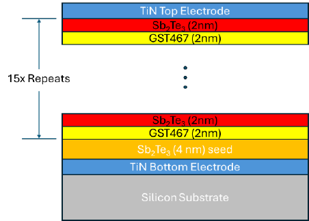
PCM Superlattice
The superlattice structure reduces the switching current (for increased energy efficiency) while also reducing resistance drift (improved stability). Their new nanocomposite exhibits a higher degree of crystallization, increasing the resistance difference between ‘on’ and ‘off’ states. This effect allows devices to be scaled smaller (40 nm demonstrated) for increased data density and to permit multiple resistance states (8 states were demonstrated). The nanocomposite also has a lower melting point, further increasing energy efficiency as well as switching speed.
The TEM image below shows one of their 40 nm PCM devices in the high resistivity (off) state. The amorphous dome can be seen in the middle of the superlattice with its interfaces.

The plot below shows that a 40 nm device GST467 deposited in a superlattice (SL) operates with a 10× lower reset current compared to a non-SL structure. This demonstrates significant energy efficiency gain with this structure.

Read more on Dr. Khan’s work here:
https://news.stanford.edu/stories/2024/01/closing-universal-memory-large-data-processing]
* Wu, Khan, et al., "Novel Nanocomposite-Superlattices for Low Energy and High Stability Nanoscale Phase-Change Memory," Nature Communications 15, 13 (2024).

AJA International’s magnetron sputtering systems offer a powerful platform for research and development in Phase Change Memory (PCM) technologies. With precise control over deposition parameters and advanced multi-target configurations, AJA systems enable the fabrication of high-quality thin films essential for PCM device structures. Researchers can reproducibly deposit key chalcogenide materials such as Ge₂Sb₂Te₅ (GST) and other compound semiconductors, supporting the development of next-generation non-volatile memory solutions. Optional substrate heating, in-situ rotation, and co-sputtering capabilities further enhance uniformity and compositional control, making AJA systems ideally suited for exploring the unique switching behavior and scalability of phase change materials.
To learn how AJA can support your PCM research, contact our sales team today.