
Thin Film Deposition Overview

Introduction to Thin Film Deposition
Thin film deposition refers to a family of techniques used to produce highly controlled material layers on surfaces. Thin layers (nanometer to micrometer thickness regime) can impart new properties to surfaces and can be used in making nanotechnology devices. The technological importance of thin films can be understood from considering the top commercial markets in which they are applied:
Semiconductors. A market whose size and importance is hard to overestimate, for which fabrication plants utilize several thin film deposition techniques to build these devices layer by layer.
Optics and photonics. Coatings enhance or enable many functions, such as anti-reflection, color filtering, and guiding propagation of light.
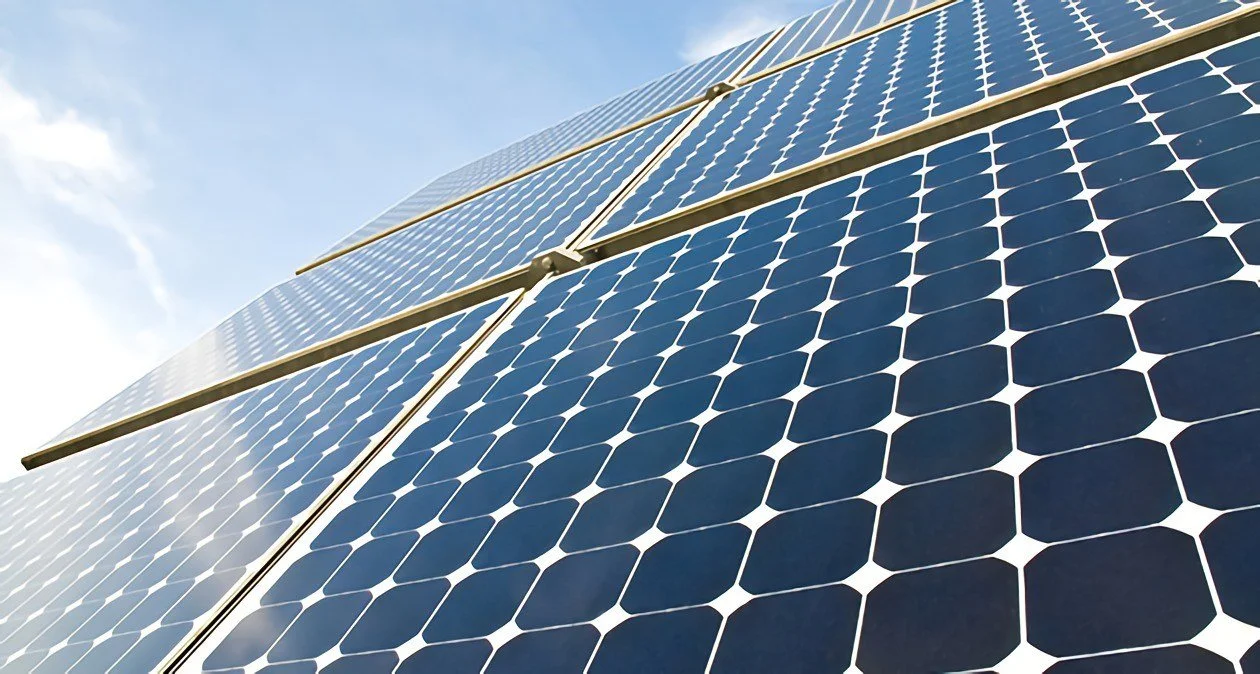
Solar cells for green energy generation. Anti-reflective and transparent conducting layers maximize performance; in some cases, the active material itself is a thin film.
Hard and wear-resistant coatings for moving machine parts and cutting tools.
Flat-panel displays and lighting. Over 300 million display tablets were delivered in 2025 alone, and patterned thin films are integral to their design.
Decorative coatings and functional surface finishes for color, corrosion resistance, and scratch resistance are found on a plethora of consumer products.
Magnetic data storage (disk drives) and magnetic field sensing.
Thin films are a critical technology in these and many more applications.
Physical Vapor Deposition (PVD) is one class of thin film growth techniques. PVD works by directly vaporizing atoms or molecules from a source of material in a vacuum chamber, allowing the vapor to condense on the surface to be coated. It can be thought of in analogy with heating water in a pot and having evaporated steam condense on the bottom side of the lid. The two most prevalent forms of PVD are sputtering and evaporation.
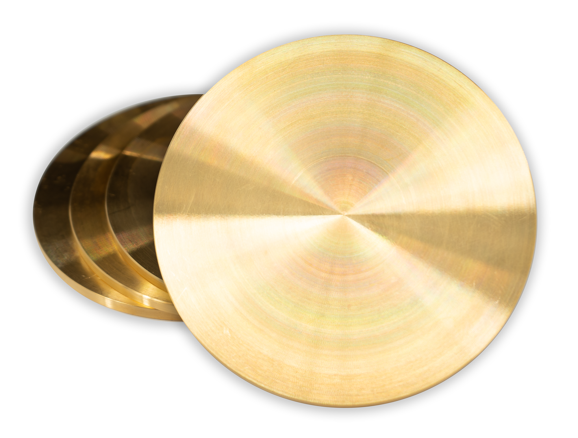
Sputtering is the process of knocking atoms out of the source material by ion bombardment. The sputtered atoms become the vapor which deposits on the remote surface to be coated. Magnetron sputtering is in turn the most common type of sputtering practiced. A magnetron sputter gun uses magnetic and electric fields to create an ion-containing plasma over the source material (target). These ions directly bombard the target, ejecting the atoms that travel to the substrate to be coated. This simple, low-cost method allows PVD from a wide range of materials, and it can be scaled from very small laboratory guns for R&D to industrial sputter guns several meters in length. AJA International provides both sputtering targets and magnetron sputter guns.

Evaporation involves heating the source material to the point where thermal excitation releases material into the vacuum, where it can transfer to the substrate. This is very much like the water vapor example mentioned above. The heat is most often supplied by either an electrically heated “boat” holding the material or by electron beam bombardment. AJA International also provides a wide variety of evaporation materials and supplies.
The array of applications is vast to create thin film coatings with these techniques. Our Applications pages provide several examples. AJA International has been providing thin film deposition equipment and support to researchers in academia, corporate R&D, and government labs for more than 35 years. We are a trusted partner and vendor of choice worldwide.
What is Sputtering?
Sputtering is a technique used to deposit thin films of a material onto a surface (substrate). By first creating a gaseous plasma and then accelerating the ions from this plasma into some source material (target), the source material is eroded by the arriving ions via energy transfer and is ejected in the form of neutral particles - either individual atoms, clusters of atoms or molecules. As these neutral particles are ejected, they will travel in a straight line unless they collide with something - other particles or a nearby surface. If a substrate such as a Si wafer is placed in the path of these ejected particles it will be coated by a thin film of the source material.
Although sputtering as described above seems relatively intuitive, familiarization with the following terms/concepts will give a more comprehensive understanding of this process.
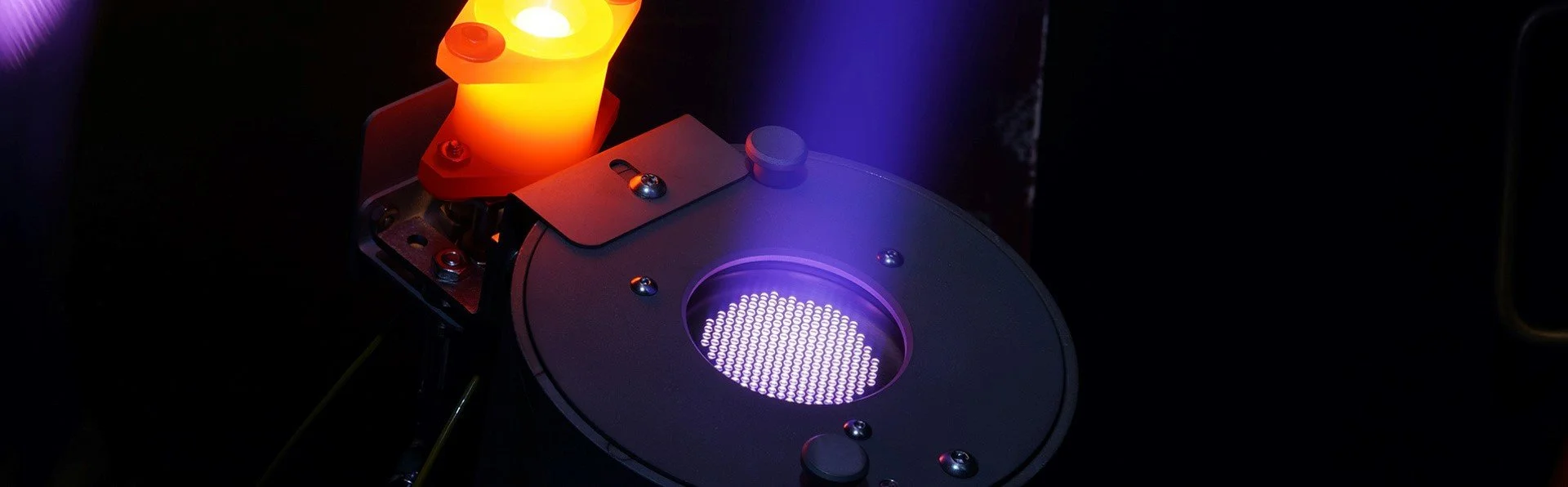
Sometimes described as the fourth state of matter (the first three being solid, liquid, gas), a gaseous plasma is actually a dynamic condition where neutral gas atoms, ions, electrons and photons exist in a near balanced state simultaneously. An energy source (e.g. RF, DC, MW electrical power) is required to feed and thus maintain the plasma state while the plasma is losing energy into its surroundings. One can create this dynamic condition by metering a gas (e.g. Argon) into a pre-pumped vacuum chamber and allowing the chamber pressure to reach a specific level (e.g. 3 mTorr) and introducing a live electrode into this low-pressure gas environment using a vacuum feedthrough.

Powering The Electrode With DC Voltage Will Result In:
1. Ever-present free electrons will immediately be accelerated away from the negatively charged electrode (cathode). These accelerated electrons collide with neutral gas atoms in their path and drive outer shell electrons off the gas atoms. This leaves the gas atom electrically unbalanced since it will have more positively charged protons than negatively charged electrons - thus it is no longer a neutral gas atom but a positively charged ion (e.g. Ar+).
2. At this point the positively charged ions are accelerated into the cathode, striking the surface and ejecting (sputtering) electrode material and more free electrons by energy transfer. The additional free electrons feed the formation of ions and the continuation of the plasma. The one-directional flow of electrons from the cathode and eventually to the substrate give this technique its name: diode sputtering.
3. All the while, free electrons find their way back into the outer electron shells of the ions thereby recombining into neutral gas atoms. Due to the laws of conservation of energy, when these electrons return to a ground state, the resultant excess energy is released in the form of a photon. The release of these photons is the reason the plasma glows.
Magnetron Sputtering
The sputtering example given above has proven to be a useful technique in the deposition of thin films when the cathode is composed of or covered with source material (sputtering target). Diode sputtering, however, has two major problems - the deposition rate is low and the electron bombardment of the substrate is extensive and can cause overheating and structural damage.
The development of magnetron sputtering dealt with both issues simultaneously. By using magnets behind the cathode to trap the free electrons in a magnetic field directly above the target surface, these electrons are not free to bombard the substrate to the same extent as with diode sputtering. At the same time the extensive, circuitous path carved by these same electrons when trapped in the magnetic field, enhances their probability of ionizing a neutral gas molecule by several orders of magnitude. This increase in available ions significantly increases the rate at which target material is eroded and subsequently deposited onto the substrate.
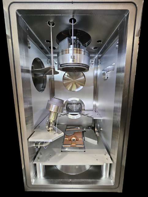
What is a Magnetron Sputtering Source?
A magnetron sputtering source is a tool to deposit thin film that mounts to a vacuum chamber by means of either flanges or feedthroughs and consists of a water-cooled cathode/target holder with an embedded magnet array and appropriate grounded shielding. Numerous designs and magnet configurations are employed to address particular requirements.
Modular Magnet Array - Magnetron Sputter Source
A modular magnet array is a special magnetron sputtering source feature developed by AJA International, Inc. in 1991 to allow the end user to convert the specific magnetic field of the source to a variety of configurations. For example, each source can be configured to operate in the:
Balanced mode to minimize substrate ion / electron bombardment.
Unbalanced mode to provide simultaneous ion bombardment to enhance film properties.
Magnetic material mode to help the magnetic field saturate and overcome the shunting effect of magnetic target materials allowing the magnetron sputter deposition of high permeability targets such as Fe.
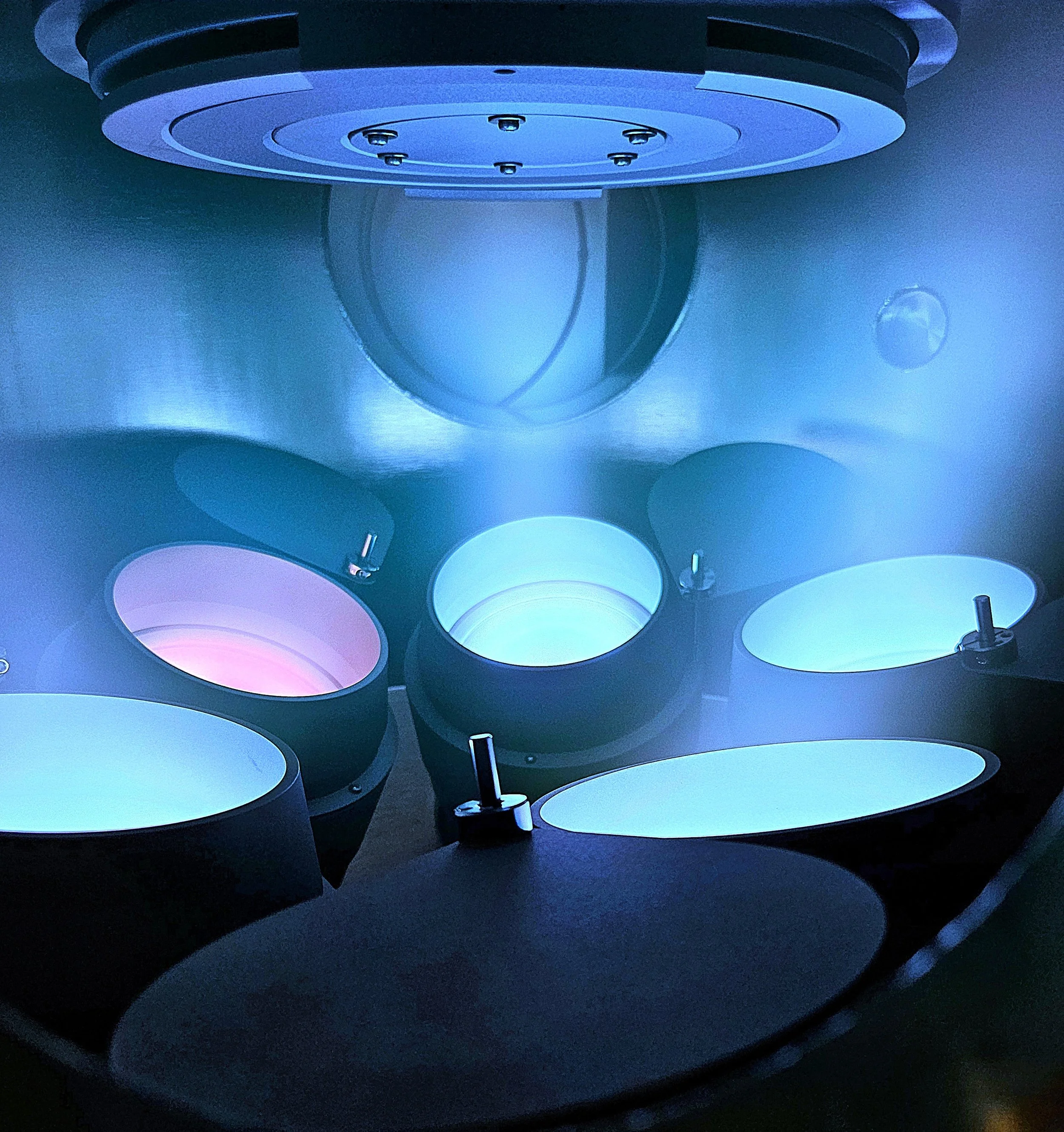
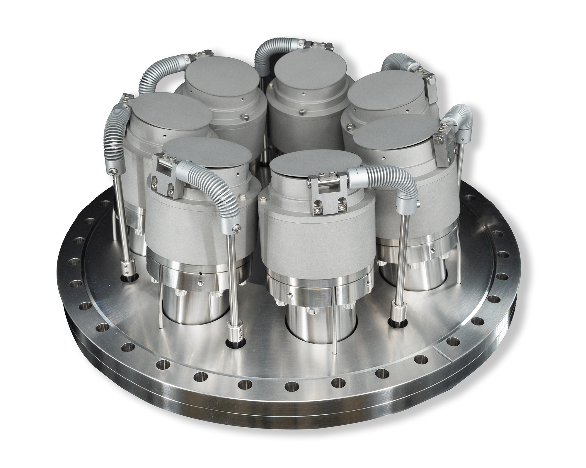
Confocal Sputtering
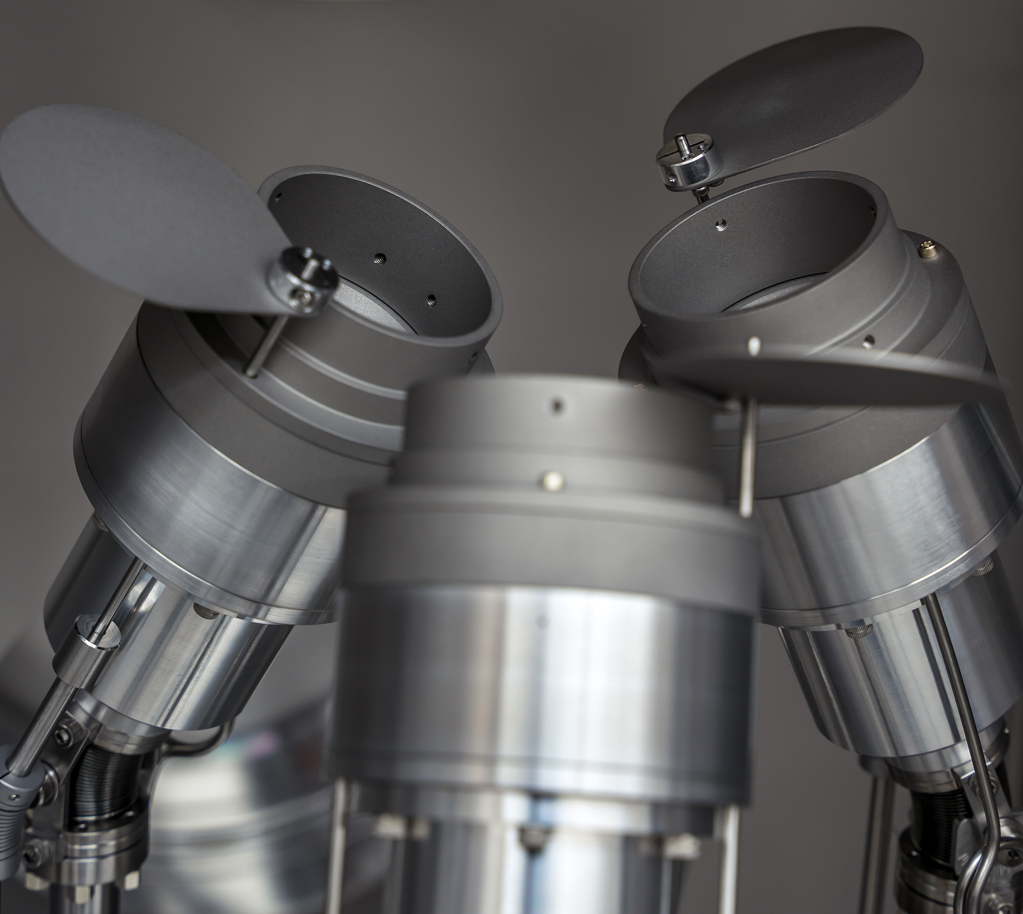
A confocal sputtering system configuration is when multiple magnetron sputtering sources are arranged in a specific circular pattern and are aimed at a common focal point. When a substrate is placed in front of this focal point and rotated on its own axis, it is possible to deposit highly uniform single layers, multi-layers and co-deposited alloy films. It is an extremely popular technique for the following reasons:
Exceptional deposition uniformity can be achieved on substrates twice the diameter of the source targets.
Ability to easily control the growth of successive layers ranging in thicknesses from less than one atomic monolayer to microns.
Minimizes time delay between subsequent layers since the substrate does not have to be re-positioned for each layer. In a confocal multi-layer deposition, every source shutter opens about one second after the previous shutter has closed thereby keeping the deposited film surface on the substrate immersed in the plasma. This keeps the interface surface free from contamination by residual gas which can block uniform deposition of the next layer material.
Complete freedom to easily grow alloys of any number of materials in any ratio with precise control. This is ideal for combinatorial chemistry applications and for optimization of compound material target stoichiometries for production applications.
The confocal sputtering configuration is compact and maintains the substrate holder in an axial orientation. This allows for much more freedom and sophistication in substrate holder design and keeps overall costs down.
For low deposition rate materials, it is possible to boost the rate by running 2-3 targets of this material simultaneously.
In-Situ Tilt Sources in a Confocal Sputtering System
In powerful R&D sputtering systems with the maximum level of flexibility, end users want the ability to operate at different working distances (distance between target and substrate). To maintain high deposition uniformity at any working distance, the focal point of the magnetron sputtering sources must be variable by adjusting the source head angle. Also, the deposition profile of materials deposited with DC, with RF, and with magnetic materials are all different, so the optimal angle for each material is not identical even if the working distance remains unchanged.
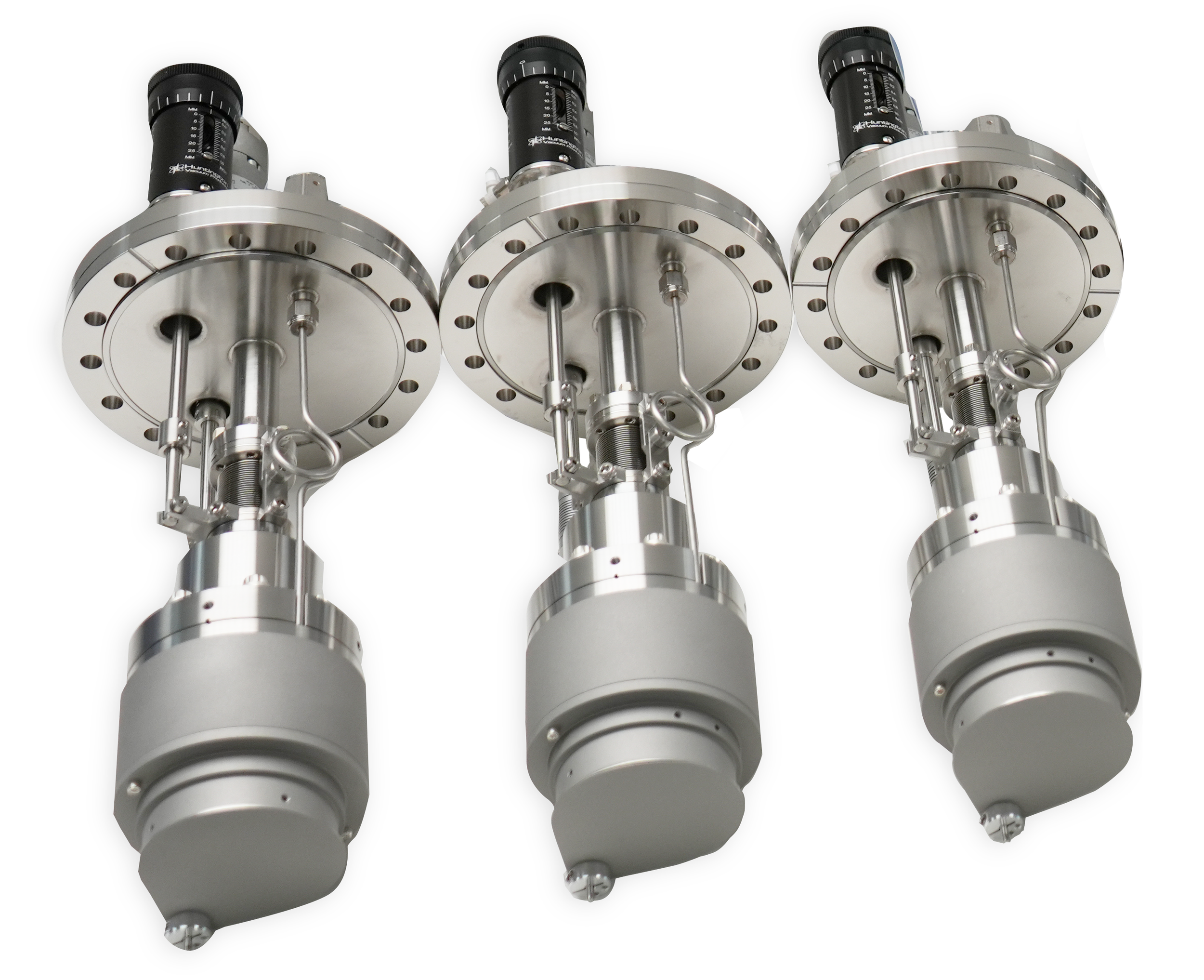
In 1991 AJA International, Inc. invented the world's first UHV and HV magnetron sputter sources with in-situ tilt. Without breaking vacuum, each source head angle could be individually set with a precision micrometer to a specific angle. If removed for service or cleaning, it could be returned to the system and set to precisely the same angle - this is much more difficult to accomplish with manually adjustable, source head tilt assemblies. In-situ tilt combined with a load-lock on the sputtering system also saves a significant amount of time in performing quick test runs in succession to find optimal source angles. What can be done in a few hours on a system with load-lock and in-situ tilt can take weeks on a system with manual source head tilt since adjustment requires venting the chamber each time to reset the angle. Finally, in-situ tilt permits the user to tilt the source away from the substrate and grow "gradient" or "wedge" films which are popular in combinatorial chemistry applications.
Direct Sputtering
A direct sputtering system configuration is when the substrate is positioned or moving directly in front of and parallel to the magnetron sputtering source targets. As a rule, target diameters (or lengths as in the case of rectangular magnetron sputtering sources) should be about 20% to 30% larger than the substrate to achieve reasonable uniformity. For example, a 100 mm wafer would require a 150 mm sputter target to achieve ± 5% deposition uniformity. Although this configuration is much less flexible and generally more expensive than confocal sputtering, it has its place in production applications which require maximum deposition rates (semiconductor wafer metallization), applications which utilize large substrates (e.g. flat panel displays) and a few techniques that demand line-of-sight deposition (e.g. lift-off).
Utilizing a direct sputtering configuration for R&D is justified in certain instances, but it is important to clearly evaluate your needs before choosing between direct and confocal deposition orientation.
What is Evaporation?
Evaporation is a technique used to deposit thin films of a material onto a surface (substrate). All materials, when heated, will transform partially to vapor. If the heating takes place in a high vacuum, the evaporated material will condense on nearby cool surfaces. If the vapor pressure is made high enough, the condensed material can form a significant layer. By placing a substrate such as a silicon wafer in the path of these evaporated particles it will be coated by a thin film of the source material.
Here we provide a more detailed description of this process and terms used.
The three common states of matter are solid, liquid, and gas. Heating a material will transition it through these three states (although some materials sublimate directly from solid to gas). However, even solids and liquids directly give off some amount of vapor. That is, individual atoms or molecules escape directly from the material, even without the entire quantity being heated to the boiling point. (Think of how water evaporates from a glass even at room temperature.) By carefully controlling the temperature of the source material (via resistive or electron beam heating), the rate of evaporation can be maintained at a desired level. Moreover, if this source material is situated in a high vacuum chamber (10-5 Torr or lower) with a substrate facing it, material can deposit on the substrate in thin film form with minimal collisions from residual chamber gas atoms. Evaporated atoms have very low kinetic energy (0.1 eV) and no ionization, so the landing energy on the substrate is lower than sputtered material. This influences the film growth.
Thermal Evaporation
The simplest and least expensive way to heat the source material to the evaporation regime is through resistive (ohmic) heating. Large capacity vacuum chamber feedthroughs bring electrical current (DC or AC) into the chamber and through a boat (a formed piece of high-temperature, resistive metal strip with a dimple to hold a small amount of source material). Low voltage, high current (a few volts and up to 300 A) power heats the boat, thus heating the source material. Vapor pressure rises quickly with temperature, so continual real-time monitoring and feedback to the power is needed to maintain a steady deposition rate. This is done by a quartz crystal monitor (QCM) which can measure the deposition rate and send a feedback signal to the system for rate control.
Thermal evaporation is typically used for lower temperature materials, due to the limitations of how hot this setup can get. A modest amount of material can be held in the boats, and they can be used a handful of times before thermal stresses cause them to break. Thus, the chamber must be opened more frequently to add material and replace boats.
More control over thermal evaporation can be had by using a furnace-type evaporator. These feature a crucible (or Knudsen cell) that can hold more material and is heated by resistive elements and features external radiation shielding. These provide more stable emission for precise control and longer operating times for a variety of materials, including organics.
Electron Beam Evaporation
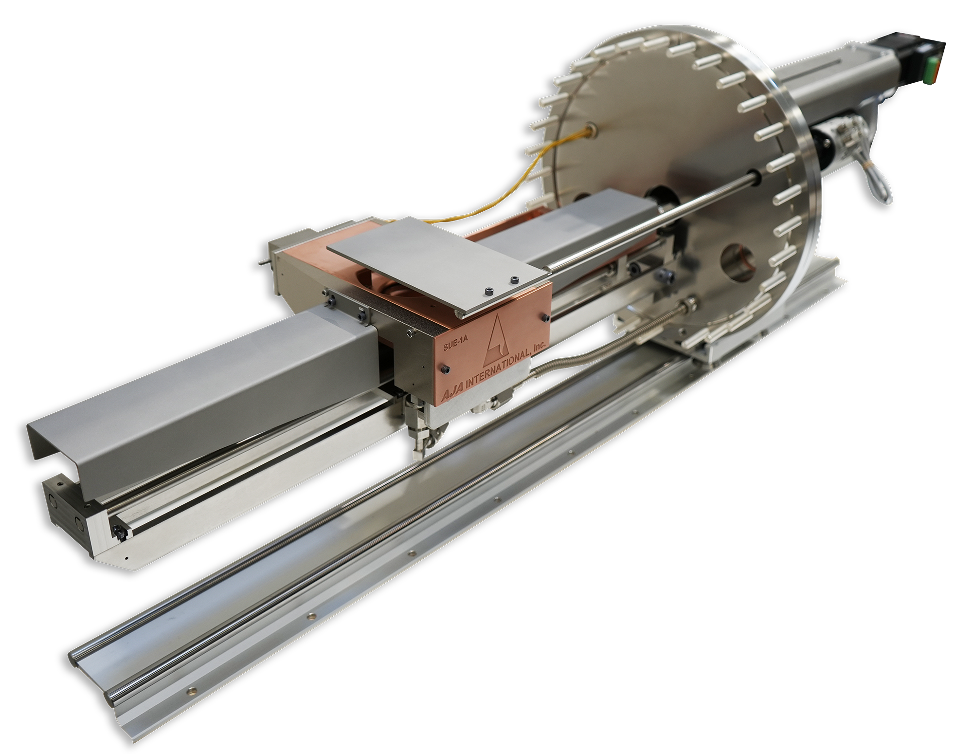
Electron beam (e-beam) evaporators use a high-power electron gun (up to 10 kW for R&D applications) to directly heat the source material. This allows depositing higher temperature materials, adds flexibility, and increases running time. (AJA International also offers in-situ crucible exchange and refill technologies, which can extend deposition campaigns further.) The base of the evaporator is a water-cooled copper block with several (e.g. six) machined crucibles (pockets) for source material. Source material, in the form of high-purity pellets, rods, or slugs is typically loaded into a crucible liner and placed in the crucible. The liner allows for clean exchange of materials. Such a configuration allows deposition of up to six materials (one at a time) from one evaporator. Crucibles may be arranged in either a circular array and indexed under the electron gun by rotation (rotary e-beam) or be arranged in a line and indexed by translation (linear e-beam). To protect the electron gun from the emitted flux, it is positioned horizontally next to the copper body where permanent magnets deflect the beam through 270° until it impinges on the source material from above. Since the electron beam diameter is small, it is also continually swept over the surface of the source material by a scan controller which drives magnetic deflection coils in the gun. There is an art in choosing scan patterns according to source material and form to get uniform heating and evaporation.
Deposition Geometry
Evaporation is arranged with the source below the substrate, since loose or molten evaporation material is held in place by gravity. E-beam evaporators and thermal boats are oriented horizontally. The throw distance from the evaporator to the substrate is much larger compared to sputtering, to get a uniform film. This is driven by the source emission characteristics. The evaporation area is typically small (cm to inch in size) and the angular distribution of the emission off-vertical has a cosine dependence. To obtain, say, ± 1% film thickness uniformity, the substrate should be a distance away of about 2.5x its width. For an 8” substrate that suggests a 20” throw distance. Since the operation does not require a process gas as in sputtering, scattering is not an issue. The longer distance also reduces the heat load on the substrate from the source material.

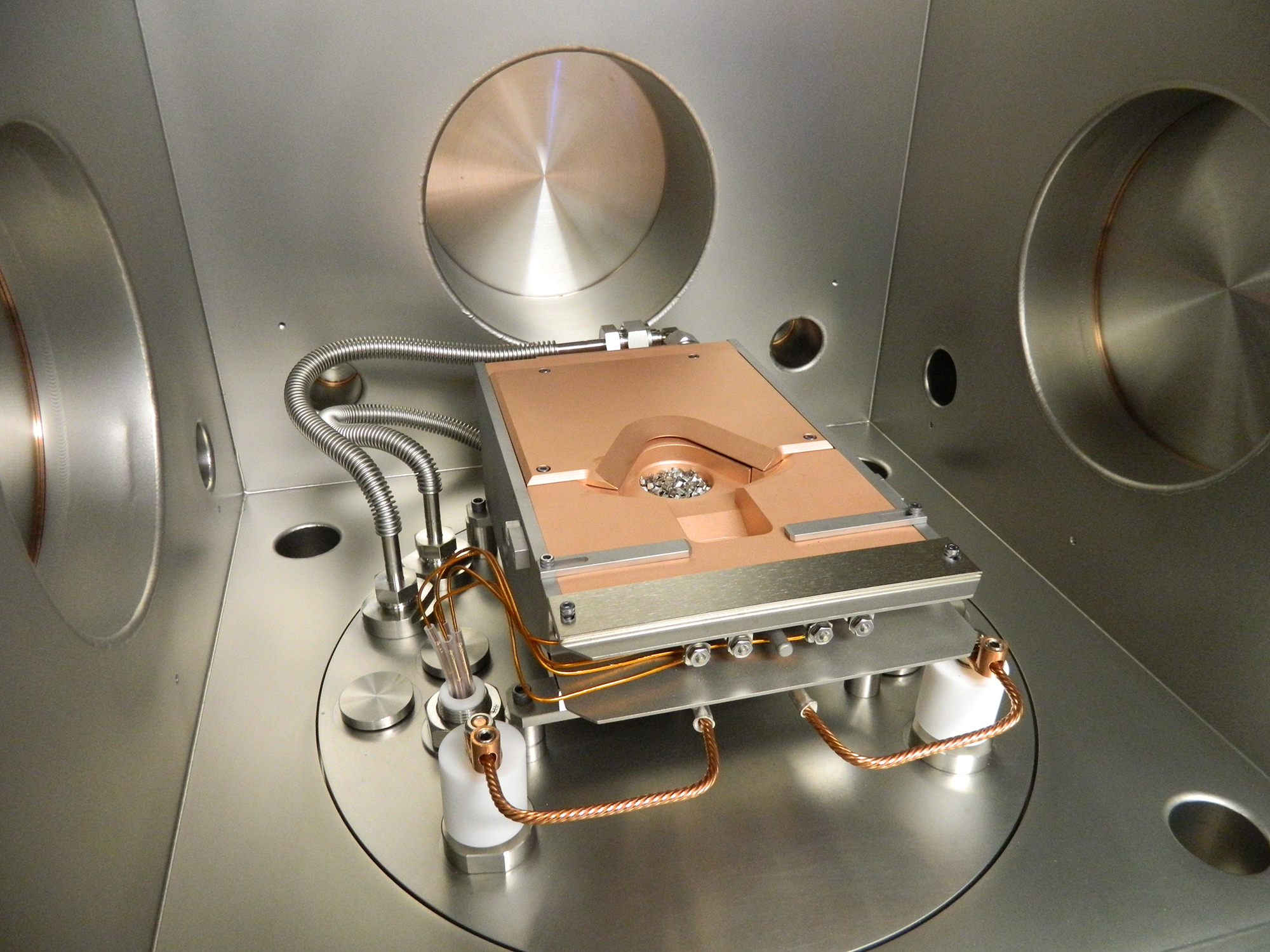
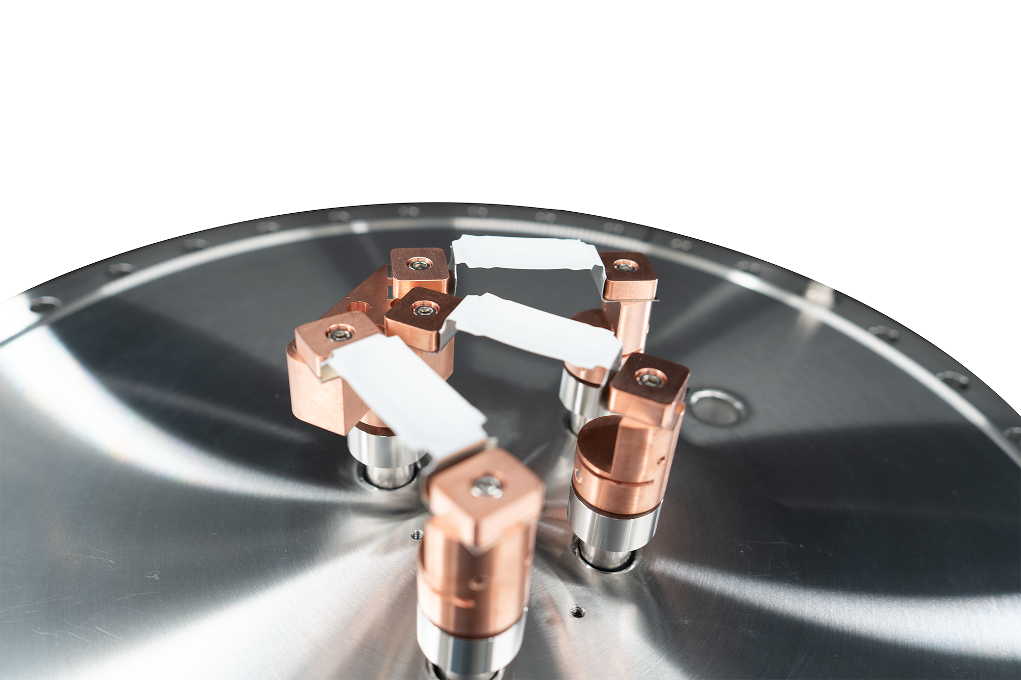
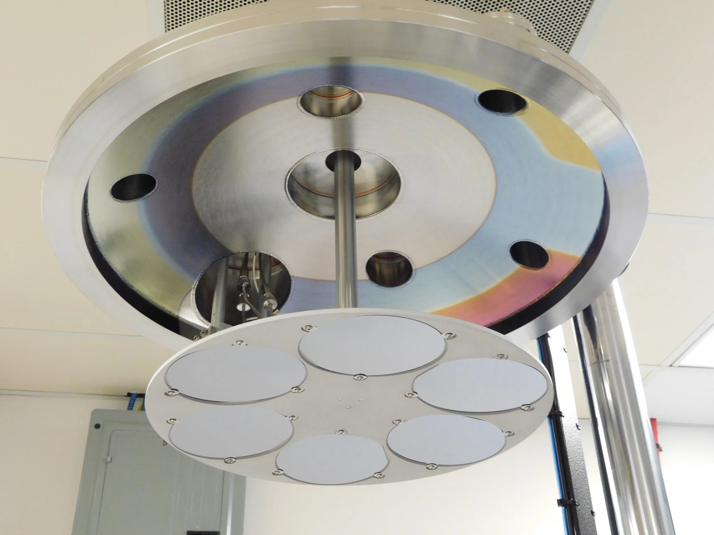
Substrate Mounting
Substrates must be mounted facing downward for coating, since the evaporators point upwards. The substrate stages feature rotation to improve film uniformity. Also, evaporators may be mounted off-axis, especially if there is more than one unit, further supporting the need for rotation. Substrate holders can also feature heating or cooling capabilities. Materials like oxides may perform better when deposited at high temperature. Hot deposition also promotes film epitaxy. Stage cooling can be used for beam sensitive substrate (e.g. photoresist-coated) or to suppress grain growth.
Some applications require the deposition flux to arrive at an oblique angle to the substrate. This may be necessary for shadow deposition or to modify the grain structure of the film. Glancing Angle Deposition (GLAD) is supported by a stage that can tilt as well as rotate. In simple cases, mounting a small substrate on an angled wedge can enable GLAD. AJA International offers tilting, rotating, temperature controlled stages that enable GLAD with tilt angles up to 90º.
Ion Assisted Deposition
The low landing energy of evaporated material, mentioned above, may not provide sufficient energy for full film densification. Ion Assisted Deposition (IAD) utilizes a low-energy ion source to bombard the growing film, providing enough momentum to surface atoms for them to reach the lowest energy atomic positions in the film. A gridded or End Hall ion source is mounted off-center pointed upward at the substrate. Ion impact promotes surface diffusion of the film atoms to densify the surface before it gets buried by the next layer of incoming material. IAD is often practiced in optics applications, as it also provides a smooth film with flat interfaces between layers and film optical properties close to those of bulk materials.