

Microfabrication by Ion Milling
Versatile Ion Milling in the Orion-IMS and 2036-IMS

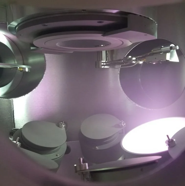
Ion milling in operation
Overview
Technologically important devices from microelectronics to MEMS to photonics to sensors – and others – are created by the physical patterning of thin films. The sensors could be passive materials, such as an accelerometer cantilever arm whose movement changes a capacitance measurement, or active materials that transduce to or from electrical signals. Well-known compounds such as Yttrium Iron Garnet (YIG) or Lead Zirconate Titanite (PZT) are examples of active materials that can be deposited as thin films and subsequently patterned in-plane to make transducers. Undercutting is often employed to release the shape from the substrate except at tether points.
In the micro- and nano-size regimes, ion milling and etching are the dominant techniques for writing patterns into films. Ion milling can operate either by physical sputtering alone or by chemical enhancement with reactive species such as oxygen. Ion milling typically starts with a plasma-based source that ionizes and then accelerates the required species to make an ion beam. Ion sources are designed to control both the beam energy and shape. Gridded (Kaufman) ion sources offer a high degree of control over the beam. These are available in a wide range of sizes. The exit grids’ potentials determine the beam current and energy, while grid shape can provide divergent, convergent or parallel beam profiles. These beam parameters directly affect the shaping of the features being milled into devices. Being a dry, beam-based technique, ion milling is highly anisotropic and thus ideal for making nanostructures. Delivered beam power of hundreds of Watts provides fast machining rates.
The broad ion beam writes a pattern into the film surface through masking. For larger feature sizes, a physical stencil mask can be placed over the device substrate to selectively remove material. For smaller dimensions, photolithography is typically utilized. Selective chemical etching creates a patterned photoresist layer whose openings define the write pattern for later milling. The photoresist may directly protect the material to be patterned, or it may be used to write a pattern to an intermediate hard mask. The substrate often needs to be cooled during operation, to prevent degradation of the organic photoresist from heating by the ion beam.
Several metrics define the fidelity of pattern transfer in ion milling: minimum feature size, maximum feature density (space between features or aspect ratio), and for the sidewalls: angle, smoothness, and re-deposited material. These are intertwined. Perpendicular beam incidence provides more vertical sidewalls, substrate rotation can smooth them, while angled deposition can be used to remove re-deposited materials from the sidewalls. Erosion of narrow photoresist lines will limit the aspect ratio of features, which may call for thicker photoresist layer. A hard mask can improve etch selectivity and depth, as can chemically enhanced ion milling. Thus, a variety of parameter adjustments are needed to create optimized structures.
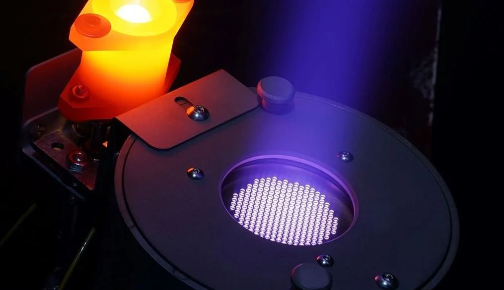
Kaufman gridded ion source with filament neutralizer
Key Features of the Orion and 2036 Ion Milling Systems for Patterning
Ion Sources:
Gridded ion sources produce a mono-energetic beam and give control over beam power. Three-grid sources can produce the lowest energy beams for milling sensitive materials such as organic layers. Sources can either have filament driven (DC) or RF-coupled plasmas. DC can be used for non-reactive milling (usually Argon), while RF opens the possibility to use either reactive or non-reactive species. Likewise, and for the same reasons, the neutralizer which injects electrons into the beam to prevent charging can also be DC or RF. Besides these options, we can also supply grid-less, filament-less, self-neutralized ion sources for reactive gas operation, such as CF4.
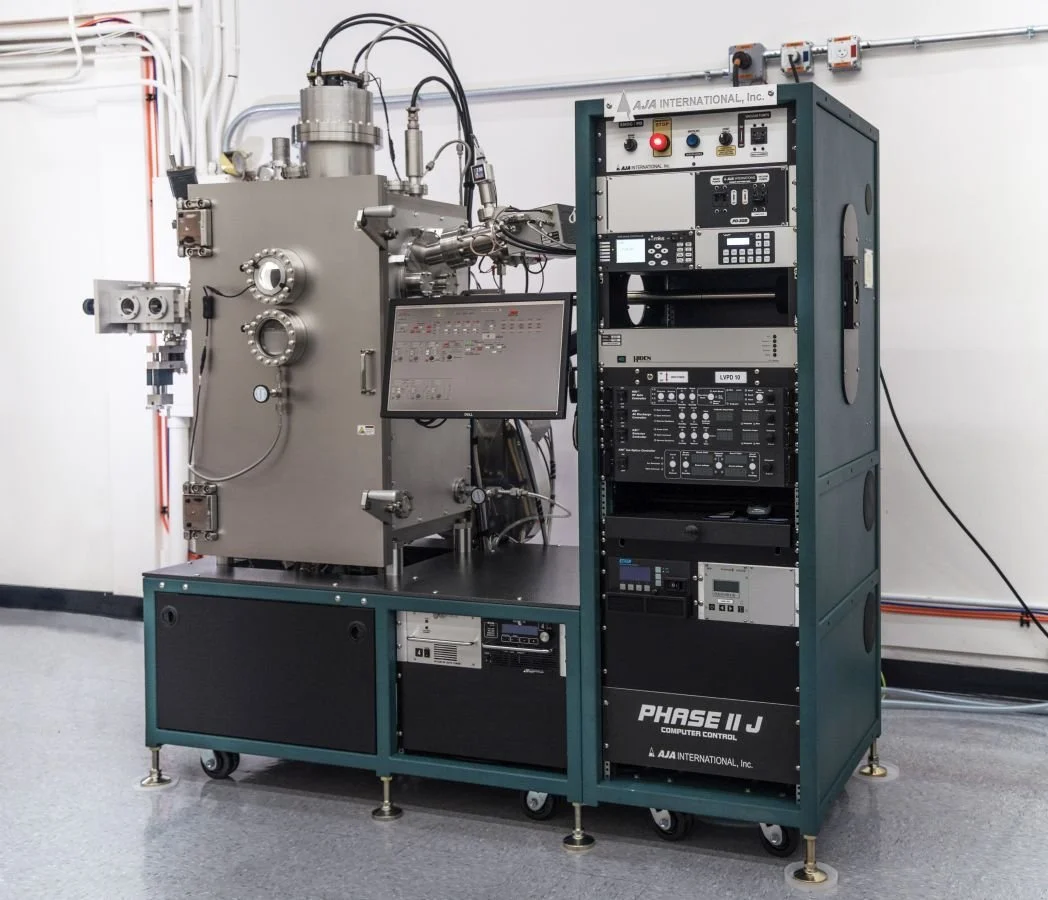
2036-IMS Ion Milling System
SIMS Endpoint Detection:
A Secondary Ion Mass Spectrometer (SIMS) can be added to detect in real time when ion milling has reached the bottom of a layer to be removed. The onset of signal from the layer beneath can trigger the software to terminate the now-complete milling operation. SIMS can also analyze film composition and inform about interfacial mixing.
Sputtering Sources:
Optional magnetron sources provide capping layers to protect device surfaces from air exposure. Substrate tilt up to ±180° is used to turn the completed device from the ion source to face the sputtering guns. Three guns can be installed, providing passivation layer options for any given run.
Explore the full range of capabilities and options for our IMS systems at https://www.ajaint.com/systems-ion-milling
Substrate Holders:
Holders for substrates up to 8” (200 mm) diameter provide compatibility with other processing equipment. Continual rotation for uniform milling and tilt up to ±90° work together to provide smooth vertical sidewalls free from re-deposit. Cooling can be provided by water, liquid nitrogen, or gas, depending on the process need.
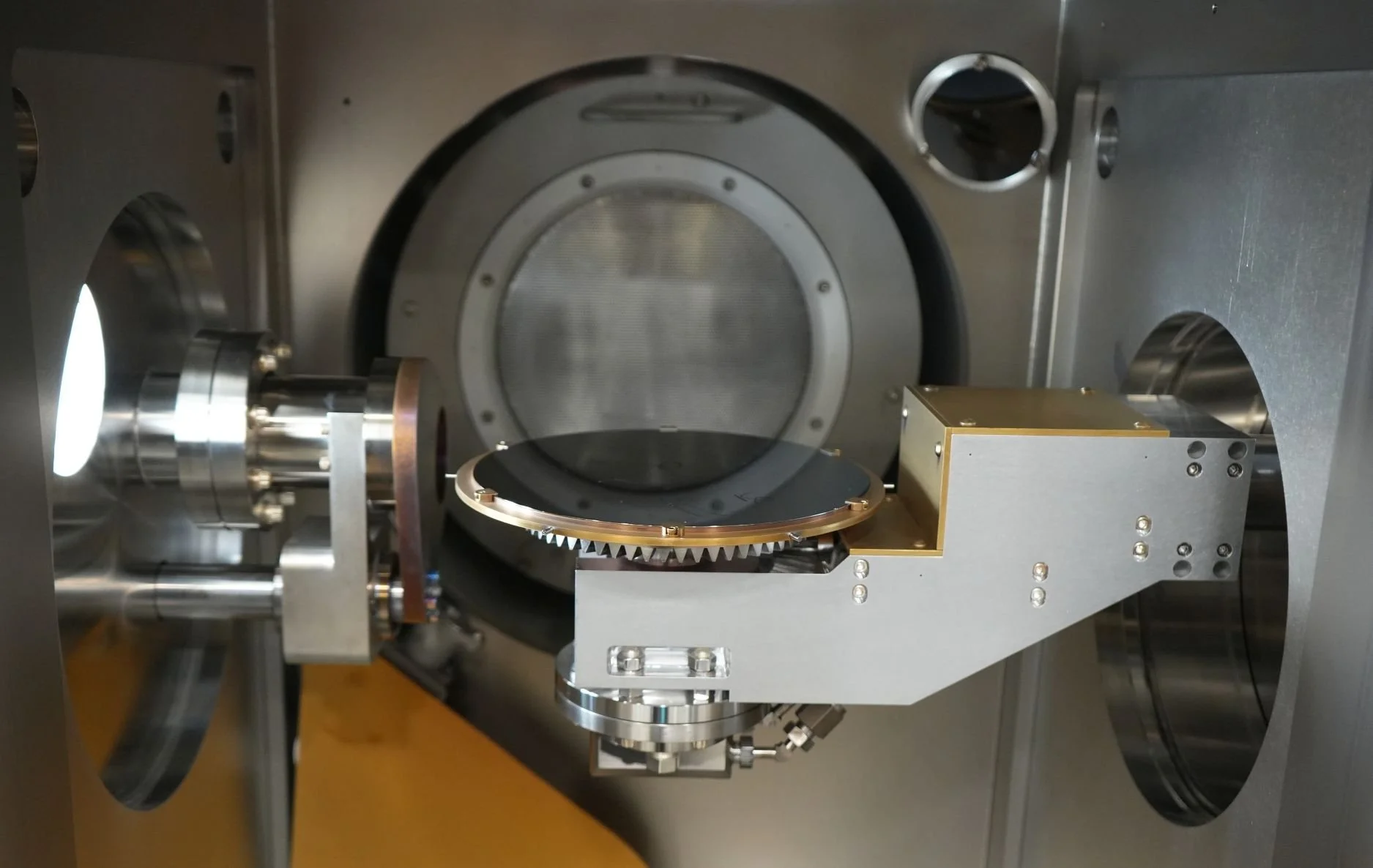
A 200 mm wafer on a rotating, tilting holder positioned at glancing angle to a 22 cm ion source.

Performance
Ion milling has a key role in the work of Professor Sunil Bhave’s group at Purdue University. They patterned bulk acoustic wave (BAW) resonators from single crystal lead magnesium niobate – lead titanate (PMN-PT) thin films [1]. The device features a disk suspended by two tethers – see image. To realize vertical sidewalls free from re-deposited material, they developed a technique dubbed CHISEL. Like a sculptor uses a series of chisels for coarse and then fine surface finishing, this cyclical process utilizes both rotation and tilt. In each cycle, milling at a tilt angle of 14° gives maximum etch rate for high throughput, then tilting to 80° faces the sidewall to the beam, removing material sputtered onto the sidewalls during the first step. CHISEL relies on the ability to program the tilt to cycle between two different values during ion milling of the PMN-PT.
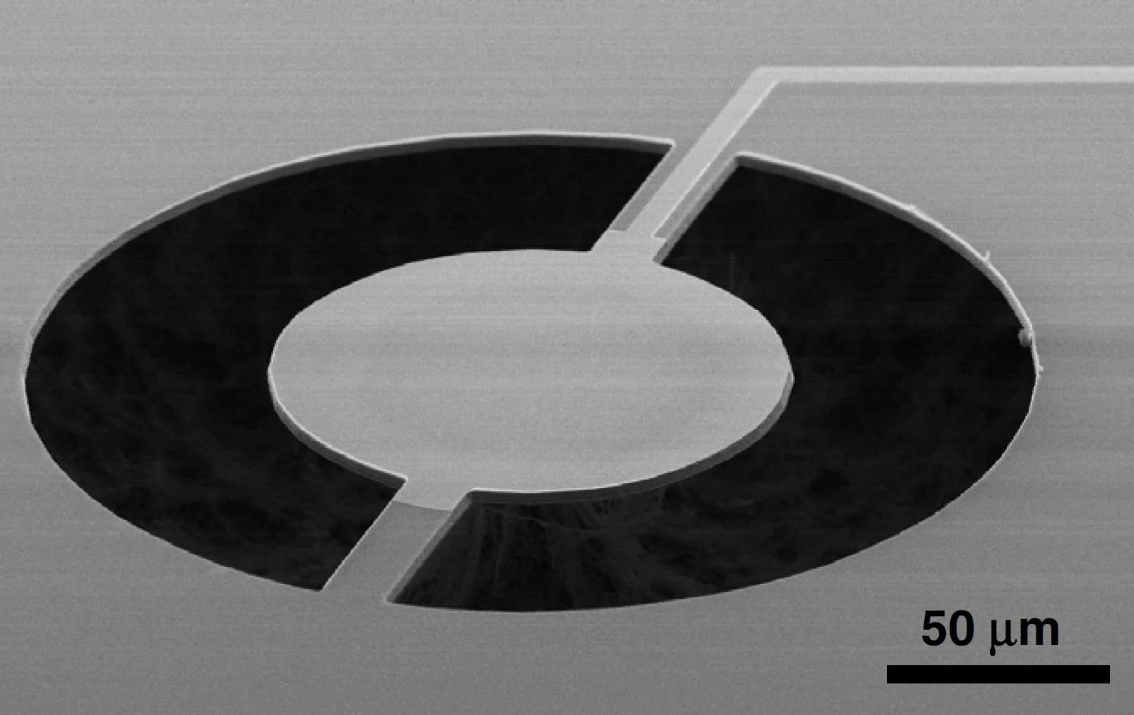
A BAW resonator
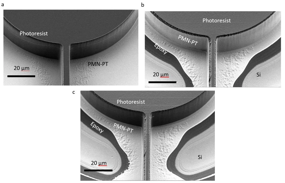
The CHISEL process (See Supplemental Note 1 of [1]). Figure shows (a) patterned photoresist on blanket film of PMN-PT, (b) PMN-PT partially etched but also re-sputtered onto sidewall, (c) removal of re-deposit.
The careful micromachining afforded by ion milling created devices whose measured resonance frequencies were well-matched to that predicted analytically and by simulation (see plot).
[1] Read the full article describing this work at: Erturk et al. Microsystems & Nanoengineering (2023) 9:52 (https://doi.org/10.1038/s41378-023-00521-3)

Resonance frequencies of BAW devices as a function of size.

AJA International’s Orion-IMS and 2036-IMS systems complete the tool set for micro- and nanofabrication. Operating along with our thin film deposition systems, their versatile milling capabilities transfer the lithographic pattern into the film for device creation and research.
To explore how AJA systems can advance your device development, contact our sales team today.